
 Focusing on compound semiconductors which are the key materials for photonic devices covering ultraviolet to infrared and superior electronic devices indispensable for wireless and optical communication as well as power electronics, we are conducting research and development on semiconductor materials and their application technologies, as well as peripheral technologies.
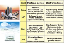
Sumitomo Electric’s compound semiconductors and their application
Compound semiconductors are widely used in various application fields in which silicon devices cannot be used. Sumitomo Electric has developed a variety of materials as a pioneer in this field.
Making use of our technologies of bulk crystal growth, epitaxial growth, simulation technique, characterization and analysis, we are promoting research and development on high-quality, cost-effective solutions for application-specific needs as well as on challenges for new materials.
Product development and key technologies
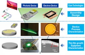 Compound semiconductors are widely used for optical devices and electronic devices. In each of these areas, we work on technological development aiming at downstream products such as epitaxial wafers, devices and modules, based on our material and device technologies.
Material design technologies
In the past, material designs depended on experiment alone. However, we are now working on simulation technologies that will help us expand our total range of R&D, such as the first principle calculation and thermal-fluid analysis technique.
We anticipate various applications, such as the creation of new materials and the development of production process.
 Green semiconductor lasers
Using our GaN substrate, we successfully developed pure green laser diodes following conventional blue-purple ones. Widespread applications including displays are expected.
GaN-based transistor
GaN also has excellent features as a substrate material for electronic devices. To make full use of its advantages, we have developed vertical transistors and now are conducting their evaluation.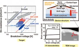 They are expected to surpass conventional silicon devices in switching speed and energy saving.
Development of semiconductor thin films
We are conducting research on the thin film growth technology of compound semiconductor crystals. Aiming at the application to near-infrared sensors for chemical imaging, light-emitting devices and advanced power Analysis of doped GaN transistors, novel thin film crystals are being developed using our nano-structural analysis.
RELATED VIDEO


Share this Post
latest post
-
 Semiconductor Processing November 26, 2023
 -
 Top Fabless Semiconductor companies October 27, 2023
 -
 Silicon Valley Semiconductor companies September 27, 2023
 -
 New Semiconductor companies August 28, 2023
 -
 List of Semiconductor companies in USA July 29, 2023
 -
 Semiconductor properties June 29, 2023
 -
 Semiconductor industry companies May 30, 2023
 -
 Canadian Semiconductor company April 30, 2023
 -
 Semiconductor companies in Europe March 31, 2023
 -
 Semiconductor jobs in Europe March 1, 2023
 -
 Freescale Semiconductor, Ltd January 30, 2023
 -
 Freescale Semiconductor Patent December 31, 2022
 -
 Freescale Semiconductor news December 1, 2022
 -
 Freescale Semiconductor stock symbol November 1, 2022
 -
 Global Semiconductor company October 28, 2022