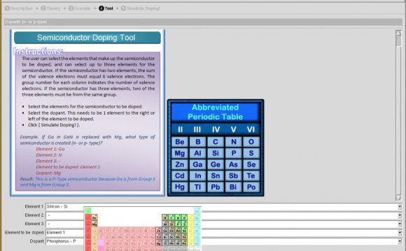
Doping is the process of adding impurities to intrinsic semiconductors to alter their properties. Normally Trivalent and Pentavalent elements are used to dope Silicon and Germanium. When a intrinsic semiconductor is doped with Trivalent impurity it becomes a P-Type semiconductor. The P stands for Positive, which means the semiconductor is rich in holes or Positive charged ions. When we dope intrinsic material with Pentavalent impurities we get N-Type semiconductor, where N stands for Negative. N-type semiconductors have Negative charged ions or in other words have excess electrons.
How Doping Works[edit]
Atoms follow a rule called Octet Rule. According to Octect-rule atoms are stable when there are eight electrons in their valence. If not, atoms readily accept or share neighboring atoms to achieve eight electrons in their valence shell. In the silicon lattice each silicon atom is surrounded by four silicon atoms. Each silicon atom share one of its electron in the valance shell to its neighbor to satisfy the octect-rule. A schematic diagram of an intrinsic semiconductor is shown in image right (Figure : Intrinsic Silicon Lattice).
Now lets see what will happen when we pop in a pentavalent element into the lattice. As you can see the image (Figure : N-type), we have doped the silicon lattice with Phosphorous, a pentavalent element. Now pentavalent element has five electrons, so it shares a electron with each of the four neighboring silicon atoms, hence four atoms are tied up with the silicon atoms in the lattice. This leaves an electron extra. This excess electron is free to move and is responsible conduction. Hence N-type (Negative Type) extrinsic semiconductor (silicon in this case) is made by doping the semiconductor with pentavalent element.
To create a P-type semiconductor, all we must do is to pop in a trivalent element into the lattice. A trivalent element has three electrons in its valence shell. It shares three electrons with three neighboring silicon atoms in the lattice, the fourth silicon atom demands an electron but the trivalent atom has no more electron to share. This creates a void in lattice which we call it has hole. Since the electron is deficient, the hole readily accepts an electron, this makes it a P-type (Positive type) extrinsic semiconductor.
As you can see at image (Figure : P-type), we have poped in boron (trivalent element) in silicon lattice. This has created a hole making the semiconductor a P-type material.
The case is no different in Germanium. Its behaves same as silicon how ever some properties do differ which makes germanium based devices used in certain application and silicon based devices used in other applications.
RELATED VIDEO

Share this Post
latest post
-
 Semiconductor Processing November 26, 2023
 -
 Top Fabless Semiconductor companies October 27, 2023
 -
 Silicon Valley Semiconductor companies September 27, 2023
 -
 New Semiconductor companies August 28, 2023
 -
 List of Semiconductor companies in USA July 29, 2023
 -
 Semiconductor properties June 29, 2023
 -
 Semiconductor industry companies May 30, 2023
 -
 Canadian Semiconductor company April 30, 2023
 -
 Semiconductor companies in Europe March 31, 2023
 -
 Semiconductor jobs in Europe March 1, 2023
 -
 Freescale Semiconductor, Ltd January 30, 2023
 -
 Freescale Semiconductor Patent December 31, 2022
 -
 Freescale Semiconductor news December 1, 2022
 -
 Freescale Semiconductor stock symbol November 1, 2022
 -
 Global Semiconductor company October 28, 2022